
USB Noise Generator: WiBo (Wireless Board)
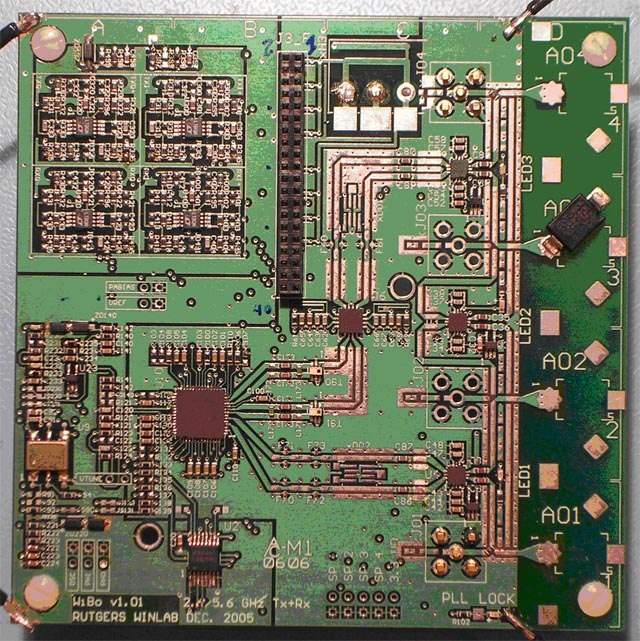
WiBo102 is a RF Front-End board designed around a Maxim, Inc. MAX2829ETN+D radio transceiver chip. This chip incorporates most of the radio functions except for the reference oscillator, baseband I/Q amps, power amps and antenna switches. The block diagram of WiBo board is show in Figure 1 with the full schematic in the attachment.

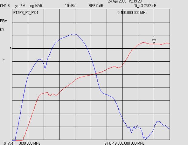
Figure 2 shows the RF power amp (AWL6951) and RF switch (upg2035) section transfer function. The AWL6951 is a dual frequency power amplifier covering 2.4 and 5.2 GHz. The blue curve shows the response of the 2.4 GHz section, the red curve the 5.2 GHz section. At 2.4 GHz, the power amplifier/switch gain is about 30dB, with power output of about 20dBm while at 5.4 GHz, the power output is about 13 dBm.

Four antennas (A01-A04) are mounted directly to WiBo102 though provision is made for adding SMA connectors and using off-board antennas if necessary. Two antennas are primarily for transmission (Tx) and two for receiving (Rx). Antenna switching is possible for diversity gain. It is also possible to switch all Tx and Rx signals into a single antenna.
A. PCB
The printed circuit board (PCB) is a 4.00 x 4.00” FR-4 four-layer controlled impedance stackup board manufactured by Advanced Circuits, Inc.. For orientation purposes, reference marks are shown along the top (A-D) and right sides (1-4) of the board in one inch increments.
Looking from the top down, the top copper layer is the component side with all the high-frequency RF transmission lines. The dielectric under this layer is 20 mils thick. The structure of the traces is coplanar waveguide with ground (CPWG). A trace width of 30 mils and gap-to-ground of 18 mils provides a very close match to a 50ohm characteristic impedance.
The next copper layer down is all ground plane. The third layer down is a signal layer with predominately vertical traces surrounded by ground plane. The fourth or bottom layer is another signal layer with predominately horizontal traces.
B. Connector J3_F and I/O
This is a 40-pin 2mm dual-inline connector which mates BaBo’s control signals, +3.3 VDC power and ground to WiBo.
BiBo’s ADC (analog-to-digital conversion) and DAC (digital-to-analog) conversion comes from an Analog Devices AD9860 MxFE processor on the BaBo board. Digital RADIO_IO_x signals come from a Xilinx Spartan 3 on BaBo.
RADIO_IO_1/¾ download programming coefficients to the MAX2829.
RADIO_IO_3/4 are shared with U2 (74HC595), an 8bit serial in parallel out shift register. U2 in turn controls five functions, namely, turn on/off of the 2GHz and 5GHz power amps, MAX2829 RXENA and TXENA signals and the MAX2829 shutdown (/SHDN).
Assuming the MAX2829 has already been programmed, to enable a TX RF output the user must program a 11001xxx into U2.
NOTE! Do not turn on both the 2GHz and the 5GHz power amps at the same time! ALSO! Do not turn on both the RXENA and TXENA lines (not sure why?).

Attachments (7)
- WiBo-lowres.jpg (190.3 KB ) - added by 20 years ago.
- WIBO103.pdf (1.7 MB ) - added by 20 years ago.
- MAX2828-9ds.pdf (1.0 MB ) - added by 20 years ago.
- MM74HC595.pdf (118.7 KB ) - added by 20 years ago.
- uPG2035.pdf (148.2 KB ) - added by 20 years ago.
-
wic2450a.pdf
(233.2 KB
) - added by 20 years ago.
Chip Antenna Data Seet
-
Amp-Switch.jpg
(37.3 KB
) - added by 20 years ago.
Amplifier-Switch Transfer Function